- MEDIA
- REPORTS
- EVENTS
- COURSES
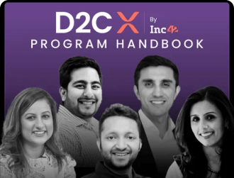 D2CX
D2CXD2CX by Inc42 is a 12-week hands-on program to help you level up your D2C game. Learn from India's top 1% D2C founders and experts through actionable insights, proven strategies and tactics on how to 10X your D2C brand.
view
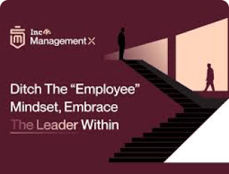 ManagementX
ManagementX by Inc42 – India’s first Startup Management Program is a 6-month hands-on program that will take you on an intense journey that shatters the outdated “employee mindset” and equips you with the “leader mindset”.
view
 D2CX Foundations
D2CX Foundations by Inc42 is a 6 week hands-on program to help you launch your D2C brand successfully and profitably. Learn from India’s top 1% of D2C founders & experts through actionable insights, proven strategies and tactics on how to launch a successful D2C Brand in 6 weeks.
view
- BRANDLABS
- ABOUT
- AI Workshop
- MoneyX Dialogues
- DATALABS